A Beginner’s Guide to Rapid Prototyping 101
- protowoerk
- Jan 26
- 3 min read
We recently came across a post in an electronics forum where a hobbyist was struggling with a PCB design—a simple USB-C board with a few LEDs powered by 5V. Despite the straightforward design, they couldn’t figure out why it wasn’t working. The problem? A short between 5V and GND that went unnoticed in their design stage. For an experienced hardware developer, it was an obvious oversight, but for someone new, it became a costly and time-consuming lesson.
At our company, we specialize in rapid prototyping for various industries. Time and again, we’ve seen how simple mistakes can lead to expensive re-spins, wasted time, and blown budgets. A PCB not only costs money to manufacture—it also takes weeks to arrive and even longer if assembly is involved. That’s why we rely on a strict pre-release checklist to ensure every design is production-ready before it’s sent out.

If you’re new to ECAD or looking to refine your workflow, here’s our ultimate checklist to minimize errors and maximize quality:
Run ERC (Electrical Rule Check)
Start with your schematic. Don’t ignore errors or warnings—every single one should be reviewed. Warnings may sometimes be acceptable, but errors must be resolved with proper solutions, not workarounds.

Export and Review the BOM
Open your Bill of Materials in a spreadsheet tool like Excel. Look for inconsistencies—like multiple symbols for the same component value or mismatched footprints. Verify component availability with suppliers (Digi-Key, Mouser, etc.) to avoid last-minute sourcing issues.

2.2k or 2k2? Looks like the same, then why other has MPN2? It was accidental but this can confuse manufacturers or they just increase the assembly cost, because they need to maintain a second component Self-Review the Schematic
Download datasheets, reference designs, and app notes for every major component. Compare your implementation against the manufacturer’s recommendations, paying special attention to pin functions and peripheral circuits.

The reference designs contains key informations for operations. E.g. the proper value/size of capacitors Peer Review the Schematic
Have a team member or colleague walk through the schematic with you. A fresh pair of eyes can catch mistakes you might have overlooked.
Implement Review Feedback
Address all findings from the schematic review before moving forward.
Run DRC (Design Rule Check) on the Layout
Just like ERC, ensure your layout is error-free. Examine every warning—some may be harmless, but others could indicate serious issues like insufficient clearance or missing connections. Review the stackup, the design rules itself.
Self-Review the Layout
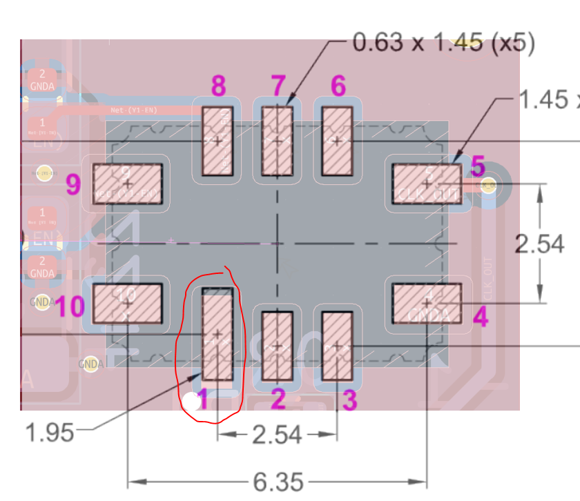
Manually check each footprint against manufacturer recommendations. Confirm pad sizes, spacing, and orientation match the datasheet.

Here the pin1 is not perfect, might cause soldering issues or other operational issues if we do not follow the manufacturer recommendation 
Manufacturers have recommendation on component layout, distances, via placement. We should follow these Generate and Inspect Gerbers
Use a Gerber viewer to verify that all layers look correct. Pay attention to copper pours, drill holes, and silkscreen alignment. Manually go over each layer.
Upload to Manufacturer & Run DFM
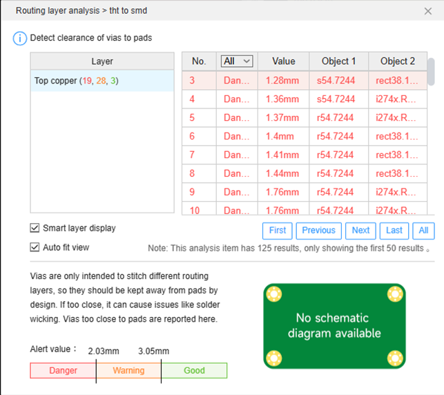
If your manufacturer offers a Design for Manufacturability (DFM) check, use it. It can flag issues like inadequate clearances, components too close to the board edge, or pads that may cause tombstoning.

Tombstoning of SMT component by using wrong footprint or routing guides not followed 
DFM shows errors/warning in the point of the manufacturer Peer Review the Layout
Have someone else review the layout—another perspective is invaluable for catching potential assembly or performance issues.

GND filling might affect RF operation. This might be skipped alone, but with another person view he can highlight it Implement Layout findings
Make necessary adjustments based on the layout review.
Package the Release Version
Create a complete design package that includes:
Project files
BOM (CSV)
Schematic (PDF)
Layout layers (PDF)
Assembly drawings (PDF)
Pick-and-place file
3D STEP file
This ensures you—or anyone else—can easily revisit or reproduce the design months or years later.
By integrating these steps into your design flow, you’ll not only reduce errors but also optimize your boards for performance, reliability, and manufacturability. At the end of the day, following best practices saves time, money, and frustration.
Do you follow a similar checklist in your workflow? What steps have saved you from a production disaster? Share your experiences in the comments below!
#ECAD #PCBDesign #RapidPrototyping #HardwareDesign #Engineering #DFM #Electronics #BestPractices #PCBManufacturing


Comments